Now You’re Playing With Power – Analysis of the AST Premium Exec 386SX laptop power and charging circuit
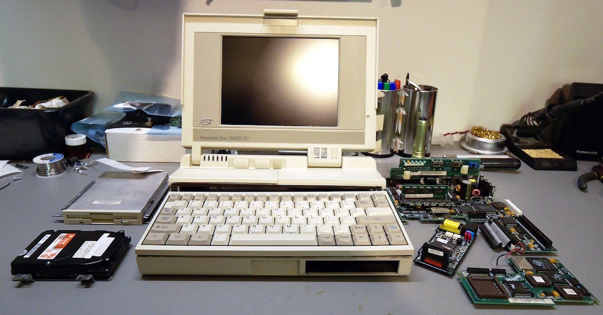
I recently bought a new laptop — an AST Premium Exec 386SX/20.
I got it from eBay for barely enough to cover shipping. The auction stated that it did not come with a power adapter, and thus, “might work, might be toast!”
As Fry (from Futurama) would say, “I like those odds!”
A thread on the Vintage Computer Federation (link here) gave me a few pointers as to what I have gotten myself into, and what potential solutions will and will not work. It became quite clear that I can’t just source a single-voltage power supply, like most laptops.
Not only is the connector not a simple DC barrel jack, but it appears there is 2-way communication between the supply and the laptop as a prerequisite to even power it up. So, it became apparent I would need to reverse-engineer the power and charging circuits on the motherboard.
Now, I tend to practice the EEVblog philosophy when acquiring new toys — “don’t turn it on, take it apart!” Devices of this age often need a little TLC, whether it’s bad caps, leaky clock batteries, or just 20 years of accumulated filth, grime, and dust. I feel a lot better applying power once I’ve given it a thorough cleaning and refurbished some prone-to-fail parts.
But, that does leave room for a touch of uncertainty if the device fails to come alive. Was it broken when I got it, or was that my contribution? So there’s always that dichotomy with which I must wrestle.
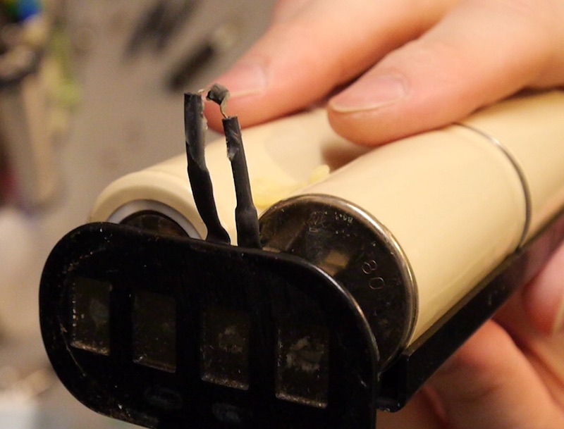
In this case, the decision is made easier by the fact that the computer arrived to me in somewhat sad shape. The plastic is actually in fantastic condition, but there is a lot of corrosion on the rear panel, and as it turns out, inside as well. Nothing too bad, thankfully, as some prior owner had clipped the leads to the RTC battery some time ago. But all of the fasteners were decaying, and there seems to be some residue indicating possible capacitor leakage. Ergo, I spent an afternoon in the company of my soldering iron, and pulled a bunch of large components off the board.
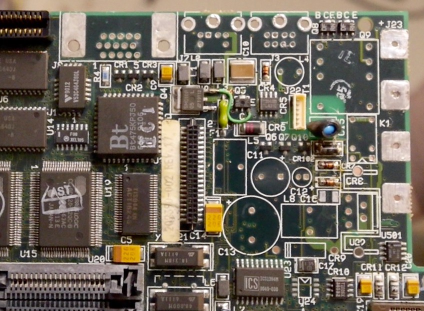
Over the course of a few afternoons and a weekend sleuthing with a magnifying glass and a continuity meter, I had a significant portion of this area mapped out in a schematic. It is definitely a work in progress, but I now have some idea of what happens through the power cable.
Since I don’t have a power adapter, and the thing is still pending surgery to fix other issues (like the corroded keyboard ribbon cable connectors), all I can see is the condition in an unpowered state. My hope is to fashion a 12-20V DC step-down converter so I can use a generic power brick. I had to find out what it would take to coax life into it, and where to inject the requisite power rail(s) first, though.
So without further ado, here’s what I’ve learned about the battery pack, the interfaces, and the circuit’s theory of operation.
The Battery Pack
For the most part, it seems to be a fairly simple machine. There is a four-conductor interface to the battery from the main board.
The bottom and top pins are Battery Negative and Battery Positive, respectively. The B- pin is also chassis ground. B+ connects directly to the four NiCad cells in series.
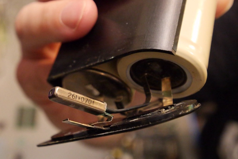
The second-from-top pin appears to be a fused link from B+. At least I think it’s a fuse. It’s a flattened metallic cylinder inside the battery pack with two flat conductors coming from it, kind of like the cell-to-cell tabs that are spot-welded in an OEM pack. It has zero resistance at room temperature.
The second-to-bottom pin seems to be a NTC thermistor. It was glued down between the two rows of cells and connects between the bottom two pins of the pack. It has about 10K resistance at room temp, and if I place it above my soldering iron, it drops rapidly to a couple K-ohms, then climbs again when cooled.
The DC Jack
The DC-In jack is an 8-pin female mini-DIN connector. Two each pins for Gnd, +5V, Batt+, and one each “TS+” and “POK”. The latter two seem to be TTL signals. POK from the supply to indicate, well, that the output power rails are OK, and my guess is TS+ is a signal from the laptop that the NTC reading is within margin. I’ll get more into those in a sec.
The laptop has a label on the back which claims a specification of 5V @ 1A, which seems kinda low. After all, according to the label on the hard drive, it alone is rated at 640mA. (Conner CP2044PK, 40MB.) That’s probably peak at startup, but still… On the other hand, a tech note I found online about conditioning the battery pack claims something on the order of twelve hours to fully drain the cells, and the main power rail traces on the PCB are pretty thin. So maybe.
The Batt+ line (from the DC In jack, not to be confused with what I will call B+ and Fused B+ from the battery) connects to the fused side of the battery pack directly, so my guess is this is a current-regulated source, not voltage-regulated. In the VCFed post linked above, someone said it measured around 8V, but that’s probably open-circuit. That would be a heck of a charge if it were capable of supplying that under load! Assuming nominal 1.2V per cell, the pack should weigh in around 4.8V, maybe a little higher freshly charged.
Theory of Operation
The laptop will draw supply from the B+ (un-fused) connection. This feeds the Normally-Closed side of a relay (K1), through the power switch on the control board (SW1), and then into a voltage regulator (U29). The regulator seems to be configured in a Boost topology, comparing the schematic with the application note (Analog Devices LT1070 Design Manual, application note AN-19). Using the formula for the feedback voltage divider, it looks to be targeting 5V output, which is to be expected.
The pass diode (CR9) cannot be disconnected from the circuit under control of the regulator in this topology, so it should follow the input voltage (minus 0.5V or so for the diode drop) at 0% duty cycle, and switch the inductor (L8) to boost it up to a steady 5V when needed — such as while the battery discharges.
When the power supply is plugged in, it feeds a PNP transistor (Q10), controlled by a NAND gate (1/4 U26, 74HC00), fed by a comparator (1/2 U501, LM393M) that is looking for a certain threshold voltage from the POK pin.
Incidentally, all this supervisory stuff is powered by either the 5V DC in, or the regulated rail (if the battery has already boot-strapped the system), which I call V+ in the schematic. The two (+5V and V+) are diode-isolated (by CR11 and CR12) and coupled into a local rail that feeds the comparator, logic gate, and some other stuff.
When the PNP transistor’s base goes low, it energizes the coil of the relay, which shunts the Normally-Open side to common, connecting the +5V DC In to the power switch and regulator. There is a bypass diode (CR102) from B+, presumably to keep the system powered if the DC In drops too low, or maybe to prevent discharging the bulk caps while the relay is switching inputs.
Side note: It’s a bit of a surprise to me that the control board power switch carries load current, rather than being a control signal, but I guess if it’s really just 1A….
There are two microcontrollers that I found which appear to have some role in the bootstrap process.
One is on the main board (U35 if I’m picking the correct designation from a few that are close together.) This is the one reading the analog input from the NTC thermistor and providing TS+ to the power adapter. TS+ seems to be active-low, since there’s a pull-up to +5V through R25.
The other is on the CPU board (U5) and controls the power and battery status LEDs via a buffer IC at U4. (That IC touts being able to deliver “high current” of 6mA source/sink on its outputs! Woohoo! We’ve come a long way since 1990.)
I suspect both of those controllers do other interesting things, but I haven’t yet attempted to trace every pin to see where it goes. Some of them can be hard to track, what with blind vias, and traces that run within inner layers of the PCB.
Up Next
There are a few particularly interesting puzzles I have not yet solved:
1) There are MOSFETs sprinkled about that appear to control local power to various regions of the board. I would like to find what is driving those gates. Not sure if this is a power-saving measure or merely power-sequencing.
2) I would like to find the master system reset circuit. My guess is it comes from the micro on the CPU board. Anyone care to place a wager?
3) I’ve read one account of a low-power alarm, but I have not yet located a battery level sense anywhere. (To be fair, I haven’t really looked.) Again, just for funsies, I would bet it’s on the mainboard micro since it appears to be the one with analog inputs. Maybe with help from the other half of the comparator IC — not sure what else that might do.
It might be educational to restore everything back to stock for a while, along with a make-shift battery pack, just to get an idea how it was originally supposed to work. I’ve been unable to find a user’s guide online, so I really have no idea how it behaves during typical charge / discharge / no battery conditions.
Backlight, or “I’m in over my head”
One final thing of note is the backlight control. I’m a bit out of my depth with that one. I am by no means a competent EE, and stuff like magnetics, high-voltage resonant switch-mode designs.. yep, that’s where I draw the line.
I did what I could to trace the relevant portions of that circuit, and it seems to be a fairly conventional CCFL driver topology. Brightness control is via one of the slider rheostats on the control board (R3), ranging from 0 ohms to 10K. It affects the adjust pin of a voltage reference IC (CR5, a tribute to the fact that it’s similar to a Zener diode), which connects to one of the pins of a 6-pin connector (J22) going into the LCD half of the case.
I am tempted to disassemble the shell and look into replacing it with a nice, easy-to-understand switching series LED driver circuit, but I am wary of biting off more than I can chew at once.
I may have forced my hand, though. While removing the transformer, the pin connected to the CCFL ballast capacitor came out of the frame and broke loose of the strand-of-hair sized winding. I have no idea if I’ll be able to repair that. I can’t even see it without help. 😉
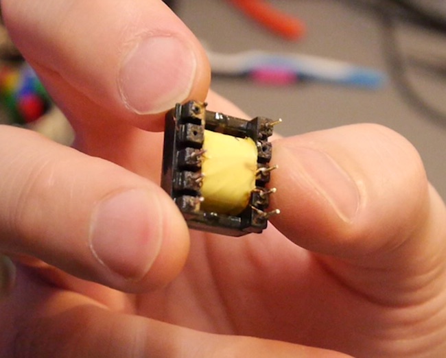
In conclusion…
Looks to me that one could just put 5V on the DC-In jack, and jumper that to POK and be all set. However, I don’t yet know what the code in either of those micros does, and they may very well keep the thing from starting up without a good thermal sense input or something reasonable on B+. There’s no telling if it was meant to run without a battery installed.
If that doesn’t work, further modification may be necessary to step-down an external power input, mimic the management controller’s normal view of the world, and maybe… just maybe even grafting in support for a pack of lithium-ion cells.
Can you imagine how long this would run with a modern battery pack the size of the original? You would only have to charge it once – ever! X-D
I really like this idea, because I think it would be fun to travel with a chonky beige 386 laptop. I might get “special treatment” going through airport security with a device nobody has been seen carrying around for 30 years, but I think it would be worth it for the side-glances from other passengers, trying to appear nonchalant as they try to hide their curiosity behind a thin and sleek tablet, while I load DOS assembly programs from a 3.5″ floppy disk.
Yes. This needs to happen. Stay tuned.
